NCP1603
http://onsemi.com
26
The PFC section is designed to operate in either DCM or
CRM. In order to keep the operation in DCM and CRM
only, the Drive Output cannot turn on as long as there is
some inductor current flowing through the circuit. Hence,
the zero current signal is provided to the oscillator/
synchronization block in Figure 67. An input comparator
monitors the Osc pin (Pin 5) voltage and generates a clock
signal. The negative edge of the clock signal is stored in a
RS latch. When zero current is detected, the RS latch will
be reset and a set signal is sent to the output drive latch that
turns on the MOSFET in the PFC boost circuit. Figure 68
illustrates a typical timing diagram of the oscillator block.
Figure 68. Oscillator Block Timing Diagram
time
clock
inductor
clock latch
(latch set signal)
Discontinuous mode
Critical mode
(latch output)
current
clock edge
Oscillator Mode in PFC Section
In oscillator mode, the Osc pin (Pin 5) is connected to an
external capacitor C
osc
. When the voltage of this pin is above
V
sync(H)
(5.0 V typical), the pin sinks a current I
odch
(9445
= 49 mA typical) and the external capacitor C
osc
discharges.
When the voltage reaches V
sync(L)
(3.5 V typical), the pin
sources a current I
och
(45 mA typical) and the external
capacitor C
osc
is charged. It is noted that there is a typical
300 ns propagation delay and the 3.5 V and 5.0 V threshold
conditions are measured on 220 pF C
osc
capacitor. Hence, the
actual oscillator hysteresis is a little bit smaller.
Figure 69. Oscillator Mode Timing Diagram in DCM
Osc pin
voltage
Osc clock
Clock edge
Drive output
(DCM)
5 V
3.5 V
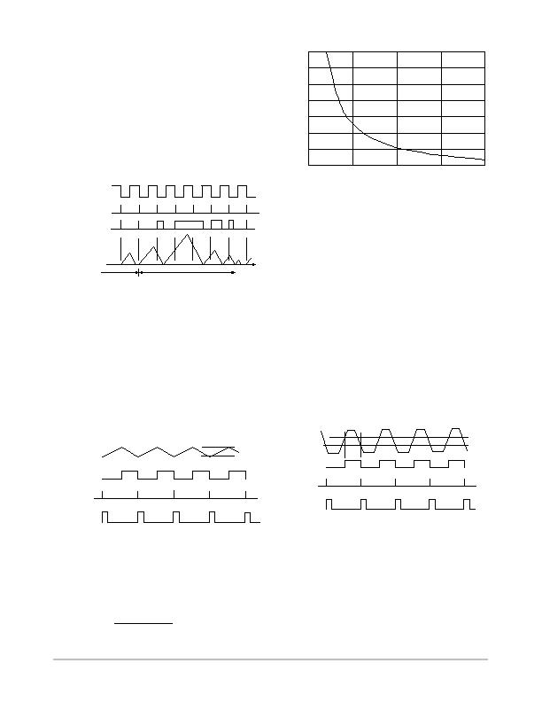
There is an internal capacitance C
osc(int)
(36 pF typical)
in the oscillator pin and the oscillator frequency is to
f
osc(max)
(405 kHz typical) when the Osc pin is opened.
Hence, the oscillator switching frequency can be
formulated in Equation 25 and represented in Figure 70.
C
osc
+
36 pF @ 405 kHz
f
osc
* 36 pF
(eq. 25)
0
100
200
300
400
500
600
700
0
50
100
150
200
f
osc
, Oscillator Frequency (kHz)
Figure 70. Osc Pin Frequency Setting
Synchronization Option
In synchronization mode, the Osc pin (Pin 5) receives an
external digital signal with level high defined to be higher
than V
sync(H)
(5.0 V typical) and level low defined to be
lower than V
sync(L)
(3.5 V typical). An internal 9.0 V ESD
Zener diode is connected to the Osc pin and hence the
maximum allowable synchronization voltage is 9.0 V. The
circuit recognizes a synchronization frequency by the time
difference between two falling edge instants when the
synchronization signal across the 3.5 V threshold point.
The actual synchronization threshold point is a little bit
higher than the 3.5 V threshold point. The minimum
synchronization pulse width is 500 ns.
There is a typical 350 ns propagation delay from
synchronization threshold point to the moment of output goes
high and there is also a typical 300 ns propagation delay from
the synchronization threshold point to the moment of crossing
3.5 V. Hence, the output goes high apparently when the sync
signal turns to 3.5 V. A timing diagram of synchronization
mode is summarized in Figure 71.
Figure 71. Synchronization Mode Timing Diagram in
DCM
Sync Signal
Osc Clock
Clock Edge
Drive Output
(DCM)
5 V
3.5 V
The PWM and PFC Section can be synchronized
together in order to minimize some of the ripple current in
the bulk capacitor as shown in Figure 72 and 73. The Out2
pin (Pin 13) is the external synchronization signal in
Figure 71 to the PFC Section. When the Out2 is in high
state, the voltage is potentially higher than the maximum
allowable voltage in Osc pin (Pin 5). Hence, a pair of
resistors divides the voltage from Out2 reduces the voltage
发布紧急采购,3分钟左右您将得到回复。
相关PDF资料
NCP1605DR2G
IC PFC CONTROLLER CCM/DCM 16SOIC
NCP1606BDR2G
IC POWER FACTOR CONTROLLER 8SOIC
NCP1607BDR2G
IC PFC CONTROLLER CRM 8SOIC
NCP1611BDR2G
IC PFC CTLR HE ENHANCED 8-SOIC
NCP1651DR2G
IC PFC CONTROLLER CCM/DCM 16SOIC
NCP1654BD133R2G
IC PFC CCM 133KHZ 8-SOIC
NCP1927DR2G
IC CTLR PFC/FLYBACK 16-SOIC
NCP380HMU21AATBG
IC CURRENT LIMIT SWITCH 6-UDFN
相关代理商/技术参数
NCP1605ADR2G
功能描述:功率因数校正 IC ENHANCED PFC CNTRLER RoHS:否 制造商:Fairchild Semiconductor 开关频率:300 KHz 最大功率耗散: 最大工作温度:+ 125 C 安装风格:SMD/SMT 封装 / 箱体:SOIC-8 封装:Reel
NCP1605BDR2G
功能描述:功率因数校正 IC High Volt Stby Mode Power Fact Corr Cont RoHS:否 制造商:Fairchild Semiconductor 开关频率:300 KHz 最大功率耗散: 最大工作温度:+ 125 C 安装风格:SMD/SMT 封装 / 箱体:SOIC-8 封装:Reel
NCP1605DR2G
功能描述:功率因数校正 IC Enhanced PFC HV and Eff Standby RoHS:否 制造商:Fairchild Semiconductor 开关频率:300 KHz 最大功率耗散: 最大工作温度:+ 125 C 安装风格:SMD/SMT 封装 / 箱体:SOIC-8 封装:Reel
NCP1605FORWGEVB
功能描述:电源管理IC开发工具 NCP1605 152 W FORWARD EVB
RoHS:否 制造商:Maxim Integrated 产品:Evaluation Kits 类型:Battery Management 工具用于评估:MAX17710GB 输入电压: 输出电压:1.8 V
NCP1605LCDTVGEVB
功能描述:BOARD EVAL NCP1605/1396 RoHS:是 类别:编程器,开发系统 >> 评估演示板和套件 系列:* 产品培训模块:Obsolescence Mitigation Program 标准包装:1 系列:- 主要目的:电源管理,电池充电器 嵌入式:否 已用 IC / 零件:MAX8903A 主要属性:1 芯锂离子电池 次要属性:状态 LED 已供物品:板
NCP1606ADR2G
功能描述:功率因数校正 IC PWR FCTR CONTROLLER RoHS:否 制造商:Fairchild Semiconductor 开关频率:300 KHz 最大功率耗散: 最大工作温度:+ 125 C 安装风格:SMD/SMT 封装 / 箱体:SOIC-8 封装:Reel
NCP1606APG
功能描述:功率因数校正 IC LO CST PWR FCTR CONT RoHS:否 制造商:Fairchild Semiconductor 开关频率:300 KHz 最大功率耗散: 最大工作温度:+ 125 C 安装风格:SMD/SMT 封装 / 箱体:SOIC-8 封装:Reel
NCP1606BDR2G
功能描述:功率因数校正 IC PWR FCTR CONTROLLER RoHS:否 制造商:Fairchild Semiconductor 开关频率:300 KHz 最大功率耗散: 最大工作温度:+ 125 C 安装风格:SMD/SMT 封装 / 箱体:SOIC-8 封装:Reel